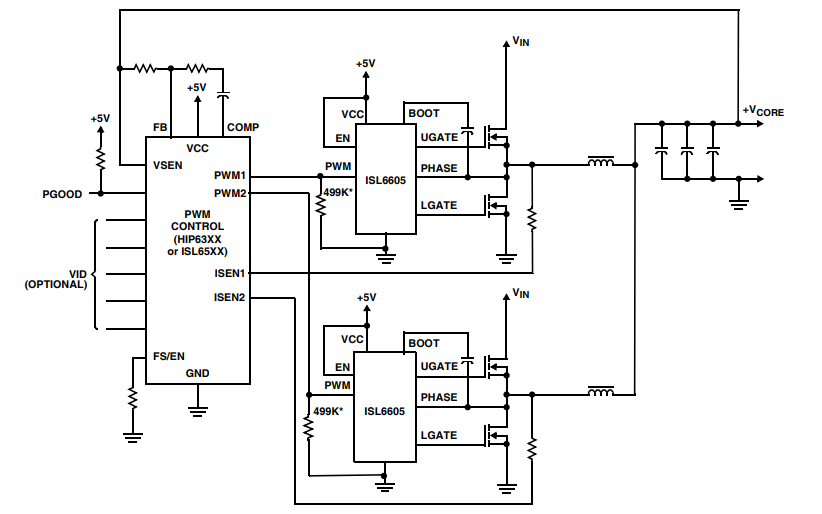
The ISL6605 is a high-frequency MOSFET driver optimized to drive two n-channel power MosFets in a synchronous rectifier step-down converter topology. The driver is combined with Intersil HIP63xx or ISL65xx multiphase step-down PWM controllers to form a complete single-stage core voltage regulator solution with high performance at high switching frequencies for advanced microprocessors.
Block Diagram

The IC is biased by a single low-voltage (5V) power supply and minimizes driver switching losses for high MOSFET gate capacitance and high switching frequency applications. Each driver is capable of driving 3000pF loads with a transfer delay of 8ns and conversion time of less than 10ns.
Typical Application

The product enables bootstrating at the upper gate via an internally guided Schottky diode, reducing implementation costs and complexity and allowing the use of higher-performing, cost-effective N-channel MosFeTs. Adaptive penetration protection is integrated to prevent two MOSFeTs from conducting simultaneously. The lower gate driver of the ISL6605 has a sink current typical of 4A and is able to hold the lower MOSFET gate during the phase node's rising edge to prevent the loss of through-power caused by the high dv/dt of the phase node.
The ISL6605 also has a three-state PWM input, which works in conjunction with an Intersil multiphase PWM controller that will prevent the output voltage from experiencing a negative transient when the output is turned off. This feature eliminates Schottky diodes, which are commonly found in microprocessor power systems to protect microprocessors from reverse output voltage damage.
Pinouts

Operation Description
The ISL6605 MOSFET driver is designed for speed and controls both high side and low side N-channel Fets via externally supplied PWM signals. The rising edge on the pulse width modulation initiates the shutdown of the low MOSFETs (see sequence diagram). After a short propagation delay [tPDLLGATE], the lower gate begins to drop. Typical descent time [tFLGATE] is provided in the Electrical Specification section. The adaptive through circuit monitors the LGATE voltage and determines the upper gate delay time based on the rate at which the LGATE voltage drops below 1V [tPDHUGATE]. This prevents the lower and upper MOSFeTs from conducting or piercing at the same time. Once this delay period is complete, the upper gate drive begins to rise [tRUGATE] and the upper MOSFETs open. The down transition on PWM indicates that the upper MOSFETs are off and the lower MOSFeTs are on. A short propagation delay is encountered before the door begins to drop [tPDLUGATE]. Similarly, the adaptive through circuit determines the lower gate delay time, tPDHLGATE. Monitor the upper MOSFET gate voltage and allow the lower gate to rise after the upper MOSFET gate to source voltage drops below 1V. The lower gate then rises [tRLGATE], opening the lower MOSFET.
Timing Diagram
