The TPIC6B273 is a monolithic, high voltage, medium current, power logic eight-way Type d latch with dmos transistor output, designed for systems requiring relatively high load power. Featuring an operating temperature range of -40℃ to 125℃, the unit includes a built-in voltage clamp at the output for induction transient protection. Power driver applications include relays, solenoids, and other medium current or high voltage loads.
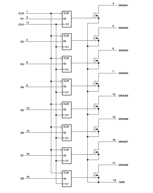
Logic diagram

TPIC6B273 contains eight positive side trigger d - triggers with direct clear input. Each flip-flop has an open drain power dmos transistor output. When clear (CLR) is high, information from the D input that meets the set time requirement is transferred to the DRAIN output on the positive edge of the clock (CLK) pulse. Clock triggering occurs at specific voltage levels and is not directly related to the transition time of the forward pulse. When the clock input (CLK) is at high or low level, the D input signal has no effect on the output. An asynchronous CLR is provided to turn off all eight dmos transistor outputs.
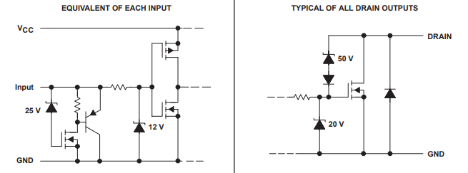
Diagram of input and output

The dmos transistor output is turned off when the given output is very low. When the data volume is large, the dmos transistor output has the capability of sinking current. The output is a low-side open-drain DMOS transistor with an output rating of 50 V and a continuous convergence current capacity of 150 ma. Each output provides a typical 500ma current limiting at TC = 25°C. The current limit decreases with increasing junction temperature to provide additional device protection.
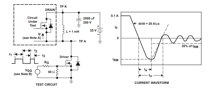
Parameter measurement information
