The LTC1100 is a high precision instrument amplifier that uses zero drift technology to achieve superior DC performance. In addition, Linear Technology is used to manufacture enhanced ltcmost silicon gate process. The input DC bias is typically 1µV, and the DC bias drift is typically 5nV/°C. An extremely low bias current of 65pA is also achieved.
Typical application

The LTC1100 is independent; That is, it achieves a differential gain of 100 without any external gain setting resistor or rectifier pot. Gain linearity is 20ppm and gain drift is 4ppm/°C. The LTC1100 operates from a single 5V power supply up to ±8V. The output is usually oscillated 300mV from its power rail with a load of 10k.
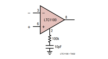
An optional external capacitor can be used from pin 7 to pin 8 to customize the device's 18kHz bandwidth and eliminate any unnecessary noise pickup. The LTC1100 is also available in a 16-pin surface mount package with a gain of 10 or 100.
Block diagram

Application program
Common-mode suppression
Due to the precise matching of internal resistances, no modifications are needed to obtain DC CMRR better than 100dB; However, as the frequency goes up, things change. Inverting amplifiers have a gain of 1.01(1.1 at gain 10), while non-inverting amplifiers have a gain of 99(9 at gain 10). As the frequency goes up, the high gain amplifier reaches its gain bandwidth limit before the low gain amplifier, reducing the CMRR. The solution is simple -- slow down the inverting amplifier to match the non-inverting amplifier. Figure 1 shows the recommended circuit. In LTC1100CS in 10x gain mode, this problem is less obvious; No need for CMRR trimming.
Improve communication CMRR

Overcompensation
Many instrumentation amplifier applications deal only with DC or low frequency signals; Thus, the LTC1100's 18kHz (180kHz at G = 10) bandwidth can be reduced by using COMP pins to reduce systemic error or reduce transmission clock noise. The feedback cap from COMP to VOUT will react with the 247k internal resistance (22.5k at G = 10) to limit the bandwidth, as shown below.
Overcompensation reduces system bandwidth

Aliasing
The LTC1100 is a chopper stabilized instrument amplifier; Like all sampling systems, it exhibits aliasing behavior at the internal sampling frequency or nearby input frequency. The LTC1100 incorporates a specialized anti-aliasing circuit that typically attenuates aliasing products by ≥60dB; However, very sensitive systems may still need to take precautions to avoid aliasing errors. See the LTC1051/ LTC1053 data sheet for more information.
Single power supply
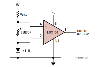
The LTC1100 will operate on a single 5V power supply, with the common model enclosure of the internal op amp including ground; Single-supply operation is limited only by the operational amplifier output swing. Internal inverting amplifiers typically have a negative saturation limit of 5mV, with the minimum common-mode limit set to 5mV/1.01(1.1 for gain of 10). Inputs can be biased on the ground, as shown below.
Low-cost bias components can be used because any errors occur as common-mode items and are rejected. The minimum differential input voltage is limited by the swing of the output op-amp. At light load, it will swing to 5mV, allowing differential input voltages down to 50µV(450µV at 10 gain). Single-power operation limits the LTC1100 to a positive differential input; A negative input will produce a saturated zero output.

Features
● Offset Voltage: 10µV Max
● Offset Voltage Drift: 100nV/°C Max
● Bias Current: 65pA Max
● Offset Current: 65pA Max
● Gain Nonlinearity: 20ppm Max
● Gain Error: ±0.075% Max
● CMRR: 90dB
● 0.1Hz to 10Hz Noise: 1.9µVP-P
● Single 5V Supply Operation
● 8-Pin MiniDIP
Applications
● Thermocouple amplifier
● Strain gauge amplifier
● Differential to single end converter