The TLC3541 and TLC3545 are high performance, 14 bit, low power, micro CMOS adc (adc) series. These devices are powered by a single 5-V power supply. Devices have single, double or single pseudo differential inputs.
Pin description

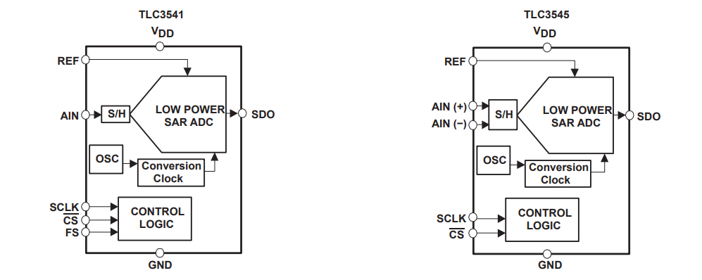
All of these devices have a Chip Selection (CS), Serial Clock (SCLK), and Serial Data Output (SDO), providing a direct 3-wire interface to the most popular host microprocessor's serial port (SPI interface). When interacted with the DSP, the frame synchronization signal (FS) is used to indicate the start of a serial data frame on pin 1 (CS) or pin 7 (FS) of the TLC3541.the TLC3545 ADC connects to the DSP only through pin 1 (CS).
Functional block diagram

The TLC3541 and TLC3545 are designed for low power consumption. Power saving features further enhance the automatic power off mode. The product family features high-speed serial connections to modern host processors with external SCLK of up to 15mhz. Both series use a built-in oscillator as the conversion clock, providing a maximum conversion time of 2.67µs.
The TLC3541/5 is a successive approximation (SAR) adc using a charge redistribution DAC. The following figure shows a simplified version of the ADC. The sampling capacitor picks up the signal on the AIN(+) pin of the AIN(or TLC3545) during sampling. When the conversion process begins, the SAR control logic and charge redistribution DAC are used to add and subtract a fixed amount of charge from the sampling capacitor, bringing the comparator into equilibrium. When the comparator is balanced, the conversion is complete and the ADC output code is generated.
